Design Your Product For EMC & Safety Right From The Start
Why “Doing It Right The First Time” Can Save You a Whole Lot of Money and Time
Lets’ face it, most of us have been there. Design a product, build what you think is the final device and then put it through approvals testing, only to discover it fails EMC, safety or worse still ESD. The result can be added costs, delays in project deliverables, a grumpy project manager and even sleepless nights. The worst scenario is that the company goes under. (My wife once worked at a technology company that went insolvent due to its inability to meet a key deliverables date due to simple preventable PCB design issues). Sure, it is great having skilled partners like Sunfire Testing to support you along the way, but ultimately it is not they who will have to re-spin a board or a product if it fails. It is you. Fortunately, there are ways to mitigate against re-spins. Prevention is usually better than cure!
I remember in my days as an engineer at IBM, the company had a catch phrase they used in the 1980’s: “Do it right the first time”. Generally, this is very true. However sometimes trial and error is a valid way to achieve the best results in a short time. But in the world of EMC and approvals, we really want to get it right the first time.
First, do your research in the dynamic world of standards. Read up on the standards, when they transition and what jurisdictions they cover. If you are unsure, contact the authorities. In Australia, our main government approvals agency is the ACMA. Sometimes test houses can also be useful, but not all of them have expertise in specific areas. It is worth consulting experts in compliance testing, such as Tim Payne at Sunfire Testing.
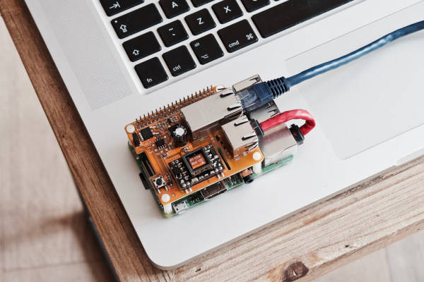
Now lets’ look at PCB design. The cost of mitigating issues up front is almost always the way to go. For example, using 0603 ferrites of negligible cost on some PCB signal lines is a lot cheaper than adding bulky and costly ferrites over cables as an afterthought. Good PCB track layout can mitigate against many other issues.
Make sure you get a capability statement from the PCB manufacturer. For example, you don’t want to be designing in track widths or clearances that are too small for the manufacturer to handle. I also recommend you get the PCBA manufacturer to panelize the PCBs. Don’t do it yourself – it is often false economy.
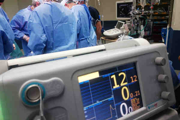
These days, the cost of using a four-layer PCB over a two-later PCB is negligible, thanks to low-cost manufacturing in China. If the board is encased in plastic, EMC may need a greater focus, especially where high slew-rate switching currents are involved. Consider issues like crosstalk and RF isolation as well as creepage and clearance. If you are driving high slew rate switching of high currents along cables, consider using low cost coax cables. I once did for a medical device which switched high current PWM driving LEDs on a board about 2 feet away. Without the coax, I was sure there would be problems. I did not even bother testing this – I just added in the low-cost cables to the design. They worked a treat and the emissions were many dB below the limits across the spectrum. If fact the entire system containing DC-DC converters and multiple stepper motor drivers passed EMC without a hitch.
Don’t forget issues where a device may need to include design items for EMC testability. For example, with the EU’s CE Radio Emissions Directive (RED), if you have a device with two or more transmitters/receivers in it (eg: Wifi and Bluetooth), you must have a way to interrogate a module’s receiver to determine the interference level to it from the other transmitter. This may be achieved with an extra comport or a pass though UART in a microcontroller, where simple queries are sent to the module using terminal emulator software like Teraterm.
If you don’t have this ability to do this on an applicable device with multiple transceivers, you won’t pass RED testing. For EMC, testability and safety, there are plenty of excellent publications on these subjects available. Some excellent publications are free on the web.
For EMC testing, I suggest if you have doubts and you plan to use a test house not in your own country for compliance, you might want to do a subset of pre-compliance in your own city. A cost-effective example might be to ensure the conducted emissions on a risky USB power input pass on a prototype PCBA. Henceforth you are increasing the chances of passing when the formal compliance testing takes place.
For IP rating “pre-compliance” testing, you can do some testing yourself. As the world is now a global village, it is relatively easy these days for the compliance testing to be performed in another country. That being said, it pays to use a knowledgeable test house that speaks your language, understands the issues at hand, and can guide you through the maze of compliance requirements.
Finally, I will leave you with a little philosophy of mine. I believe for most PCBA designs, it is normal to do a re-spin during the development phase beyond the primitive prototyping stage. Expect it and plan for it. If you avoided a re-spin, just consider you got a bonus. If there are two or more re-spins for reasons such as marketing requirement changes, unexpected end-of-life components, circuit signal quality issues or reliability issues, then it is worth doing a review of what could have been done better to prevent these extra re-spins in future.
Contact The Author For Help With Your Next Project
David Byrne, Nine Dots Technology, www.ninedotstech.com.au

We make compliance testing easy.
Submit your project details today for a no-cost quote
Request Quote